

high-quality AIN compound
semiconductor material
L&D INC.Our Product
AlN-Template on Sapphire
For UVC LED & UVC Sensors
2inch AlN on Sapphire Template
2inch AlGaN on AlN/Sapphire Template
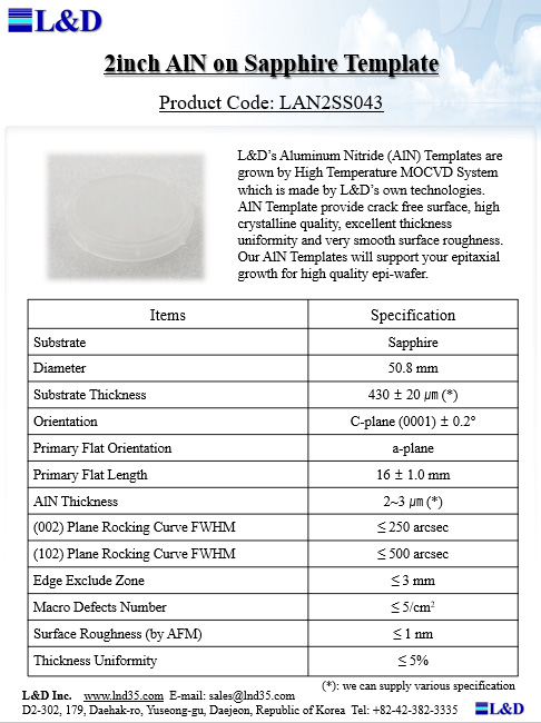
2inch AlN on Sapphire Template
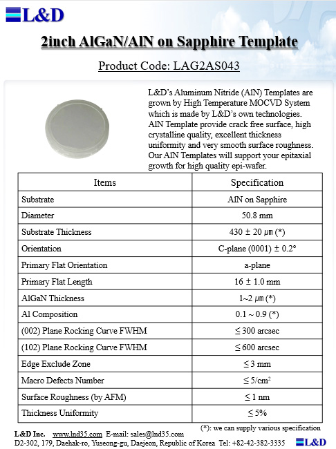
2inch AlGaN on AlN/Sapphire Template
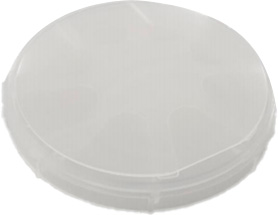
4inch AlN on Sapphire Template
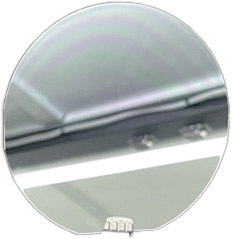
4inch AlN on SiC Template
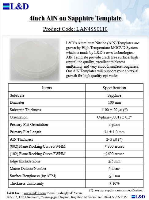
4inch AlN on Sapphire Template
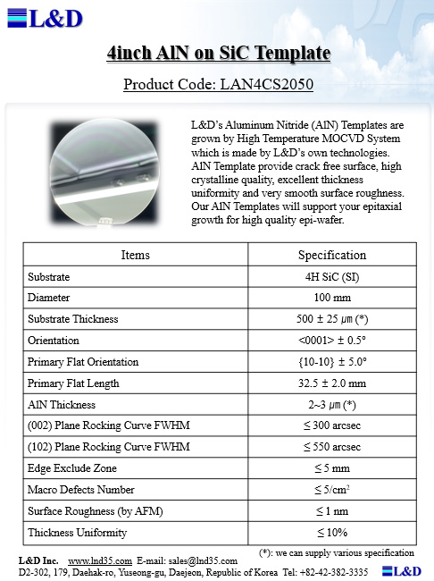
4inch AlN on SiC Template
High Performance
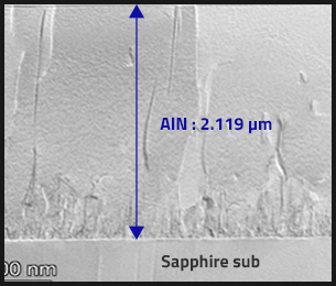
TEM Image
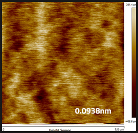
AFM Data
Our Technology
Using the own designed high temperature MOCVD.
Design of MOCVD, an essential equipment for epi-wafer manufacturing
L&D's Vision
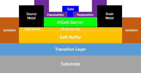
Commercial structure
GaN-Buffer layer
L&D,
substitution
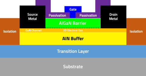
L&D’s structure
AIN-Buffer layer
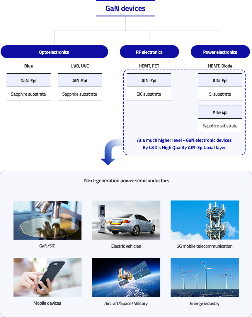
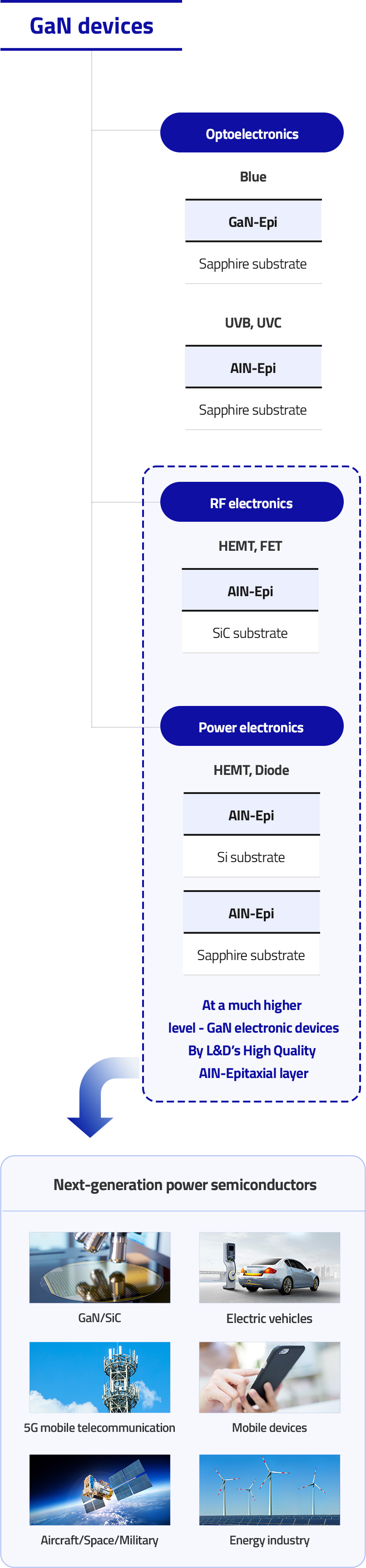
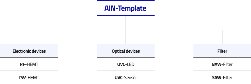
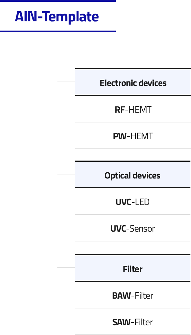
Uses of AIN-Template
Key properties of AIN (vs. other materials)
| Material | Thermal Expansion Coefficient (ppm/°K) | Thermal Conductivity (W/㎝·°K) |
|---|---|---|
| GaN : gallium nitride | 5.6 | 1.3 |
| AIN : aluminum nitride | 4.3 | 2.8 |
| Si(111) : silicon | 3.6 | 1.5 |
| SiC : silicon carbide | 4.2 | 3.9 |
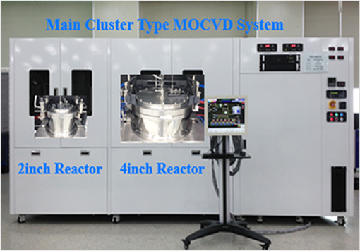
MOCVD System
- Batch size
- 8pcs/4” ,18pcs/2” (HT-MOCVD)
- Growth temperature
- 1400°C or lower
about MOCVD
A type of chemical vapor deposition (CVD) technologies forming a thin film over the surface of high temperature substrate
Patent registration and application status
| Registration date | Title of the rights | Registration number |
|---|---|---|
| 2014. 06 | Multi Chamber Substrate Processing Apparatus using Robot for Transferring Substrate | 10-1409752 |
| 2017. 08 | Shower head and device for manufacturing a semiconductor substrate having the same | 10-1765754 |
| 2016. 12 | SUBSTRATE PROCESSING APPARATUS | TW.I560797 |
| 2017. 05 | CHEMICAL VATPOR DEPOSITION APPARATUS WITH HEAT SHIELD | ZL201210295798.8 |
| 2021.11 | Active semiconductor devices | 10-2021-0156634 (Application number) |
Company
L&D Inc.
L&D Inc. is an epitaxial wafer specialist
founded by semiconductor experts
with more than 30 years of experience
Our goal is to become the market leader
with our expertise in compound semiconductor epi-wafers,
a key component in electronic devices
and UVC opto-devices, predicted to be in high demand.
Company profile
- Company name
- L&D Inc.
- Core business
-
Manufacture of AIN-based compound semiconductor epi-wafers
Development of growth and manufacturing technologies of epitaxial wafers
- Contact
- talk@lnd35.com
+82 42 382 3335
Locations
- Headquarters
- Research center
179, Daehak-ro, Yuseong-gu, Daejeon, Republic of Korea, 302 (Dajeon Startup Park)
80, Daehak-ro, Buk-gu, Daegu, Republic of Korea (Kyungpook National University, Daegu Campus. Semiconductor Research Bldg.)